In this lab we learned how shift registers work and how they can be used to control eight outputs at a time while taking up only a few pins on your micro controller. This is done using a thing called "synchronous serial communication" which allows you to pulse one pin up and then down allowing you to communicate a data byte to the register bit by bit. Once the whole byte is transmitted the HIGH, LOW messages located in each bit are then transmitted to its corresponding output pin. Here is a diagram of the shift register we used for the lab:
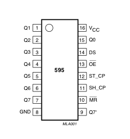 | PINS 1-7, 15 | Q0 " Q7 | Output Pins |
| PIN 8 | GND | Ground, Vss | |
| PIN 9 | Q7" | Serial Out | |
| PIN 10 | MR | Master Reclear, active low | |
| PIN 11 | SH_CP | Shift register clock pin | |
| PIN 12 | ST_CP | Storage register clock pin (latch pin) | |
| PIN 13 | OE | Output enable, active low | |
| PIN 14 | DS | Serial data input | |
| PIN 16 | Vcc | Positive supply voltage |
Our overall goal for this lab was to control a seven segment LED counter using . We had a few problems while trying to figure out what pins controlled what on the counter but after we discovered that it was a common anode counter it was smooth from then on. We were able to control the counter by using only 3 pins in our arduino.
No comments:
Post a Comment